


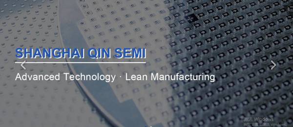
Shanghai QinSemi Technology Co., Ltd與我司簽訂網(wǎng)站建設(shè)協(xié)議
日期 : 2023-09-10 18:03:41
As one of the building blocks of “more-than-Moore” era, compound semiconductor e.g. III-V or II-VI materials play a very critical role as substrate materials of electronic/electric chips. Compared with traditional silicon substrates, these compound semiconductor materials hold special physical and chemical properties such as large bandgap, high carrier mobility, resistivity to radiation, optical transparency et al. Many innovative structures and chip designs take those advantages to realize miniaturization, low cost and high performance, which makes a business success possible. A good example is the electric vehicles (EV) equipped with a bunch of high-voltage chips made of silicon carbide (SiC) substrates, high-speed re-chargers are also taking benefits from the SiC chips. In the era of “post-Moore”, technology development of compound semiconductors triggers more commercial attempts, furthermore their business success or potentials motivate massive investment in developed economies. Rich investment results in the boost of markets and shorten lab2market period. This positive feedback could easily be observed in China. The high demand and technical requirement from downstream customers promote mass production of high-quality compound semiconductor substrates and wafers, with fast iterations of technology improvement.
網(wǎng)站建設(shè)
網(wǎng)站建設(shè)
 相關(guān)文章
 精彩導(dǎo)讀
 熱門資訊
熱門資訊